
Revolutionizing PCB Design: How AI Will Propel Us into a New Era of Efficiency
- Gulshan Sharma
- May 26, 2025
- 4 min read

The world of Printed Circuit Board (PCB) design is on the verge of a significant transformation, driven by the rise of Artificial Intelligence (AI). As our electronic devices grow in complexity and demand for efficiency increases, embracing AI in the PCB design process becomes essential rather than optional. This shift promises to streamline workflows, inspire creativity, and usher in a new era of innovation in the electronics industry.
Understanding the Current State of PCB Design
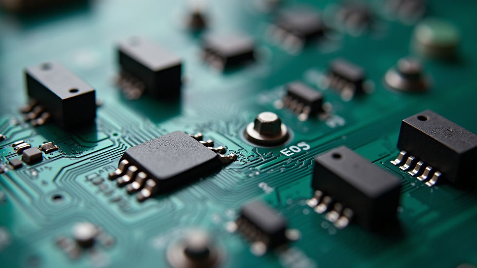
The traditional PCB design process often involves manual annotations, repetitive iterations, and slow workflows. Designers depend heavily on their skills and intuition, constantly trying to balance functionality, manufacturability, and design constraints. These challenges result in longer timelines and escalating costs that can stifle innovation.
In a fast-paced tech environment, companies seek ways to speed up time-to-market by introducing tools that allow for quicker prototyping and design validation. For example, studies indicate that design cycle times can be reduced by up to 30% when using automated tools.
The Emergence of AI in PCB Design
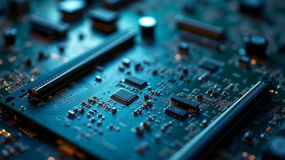
AI technologies are changing how design teams tackle PCB layouts. By utilizing machine learning algorithms and data analytics, AI can optimize design choices based on extensive datasets. For instance, AI can analyze thousands of previous designs, learning from earlier successes and failures to avoid potential pitfalls. This capability significantly shortens design cycles and opens up more options than ever before.
For example, an AI system might suggest an alternative layout based on data from a prior project, potentially saving a company thousands of dollars in material costs and reducing the likelihood of design rework.
Enhanced Efficiency Through Automation
The most notable benefit of AI in PCB design is the automation of mundane and repetitive tasks. AI can take care of component placement, routing, and error-checking. This allows engineers to concentrate on more creative and strategic decision-making. Automating these tasks not only accelerates the design process but also minimizes human error.
For example, tools powered by AI can adjust design parameters in real-time, suggest alternative layouts based on design goals, and avoid potential production issues by analyzing historical data. As a result, PCB designers achieve greater precision and consistency, with research indicating a 20% reduction in costly revisions due to automation.
Improved Collaboration and Design Iteration
AI fosters better collaboration among design teams. Cloud-based platforms integrated with AI enable multiple engineers to work on the same project simultaneously, regardless of location. This promotes a more flexible environment where real-time feedback can enhance the design process.
AI tools can improve communication by allowing designers to share insights derived from data analytics. This approach creates a more iterative process, where designers continuously refine their work based on AI-generated inputs. Such collaboration can lead to stronger, more efficient end products.
The Role of AI in Simulation and Validation
Testing and validation play vital roles in PCB design and can be greatly improved by AI. Traditional simulation methods are often slow and may overlook subtle design flaws. In contrast, AI can conduct simulations more quickly and accurately, utilizing past data and predictive algorithms to identify potential electrical and thermal issues.
For example, imagine a scenario where AI simulates various loads on a circuit board, allowing engineers to uncover weaknesses before they produce physical prototypes. This proactive approach can reduce failure risks and lower costs associated with late-stage design changes.
Challenges and Considerations
While the potential for AI to enhance PCB design is vast, it comes with challenges. There is a learning curve associated with adopting new AI tools, and engineers must familiarize themselves with these technologies to leverage their full potential. Additionally, integrating AI into existing workflows often requires significant changes in mindset and processes.
Reliance on data integrity is another important factor. AI systems function best with high-quality, relevant data for training. If the data is flawed, there is a risk of compounding errors, which can complicate, not simplify, the design process.
Looking Ahead: The Future Landscape of PCB Design
As AI continues to develop, we can anticipate even more groundbreaking changes in PCB design. In the future, we may see fully automated design systems capable of generating layouts based solely on specified requirements. Picture a scenario where engineers provide input, and AI manages the design, optimizing performance, manufacturability, and cost—all while maintaining quality.
Additionally, as AI technology advances, we may also benefit from enhanced predictive analytics, allowing design teams to anticipate market trends and consumer needs better.
Embracing the Wave of Change
The integration of AI into PCB design signifies an exciting shift toward a more efficient, reliable, and innovative future within the electronics sector. By automating routine tasks, improving collaboration, and streamlining testing processes, AI has the potential to reshape how PCB designers operate.
For organizations to thrive in this new era, it is essential to invest in training and technologies that maximize the benefits of AI. The road ahead is full of potential for those willing to embrace change, ensuring that the future of PCB design is not only efficient but also revolutionary.


Comments