
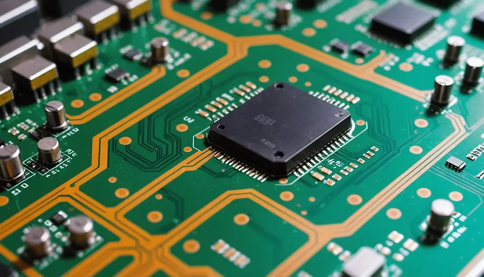
Critical Gaps in India's PCB Fabrication Ecosystem
- Gulshan Sharma
- May 8, 2025
- 2 min read

Lack of Confidence in 4-Layer and Above PCB Fabrication
While there are a few manufacturers offering 4-layer PCBs, consistency, yield, and reliability remain concerns.
There’s a gap in process maturity and quality control for multilayer (>4-layer) boards used in high-speed and high-density applications.
India lacks quick-turnaround prototyping and low-volume high-complexity PCB fabs—a must for R&D-intensive sectors.
Widespread Support for Blind and Buried Vias
Technologies like blind vias (connecting outer layers to inner layers) and buried vias (connecting inner layers without touching outer layers) are essential for HDI (High-Density Interconnect) PCBs.
Most Indian fabs are not equipped with laser drilling, X-ray drilling alignment, or sequential lamination processes required for these advanced interconnects.
As a result, telecom, medical, and defense OEMs continue to import such boards from Taiwan, China, or Japan.
Absence of HDI (High-Density Interconnect) Capabilities
HDI PCBs enable smaller form factors, faster signal transmission, and higher pin count—all essential for smartphones, wearables, and IoT.
India lacks the fine-line etching (<50 μm) and microvia fabrication expertise required for HDI production.
Very few Indian fabs can offer 1-2-1 or 2-4-2 stack-up HDI configurations at commercial scale.
No Domestic Facilities for Flex and Rigid-Flex PCBs
Flexible and rigid-flex PCBs are key to foldable devices, automotive electronics, and medical wearables.
India has negligible presence in this segment. Fabrication requires polyimide substrates, roll-to-roll equipment, and precision lamination, all of which are missing or underdeveloped.
Limited Support for Embedded Components and Embedded Capacitance
Advanced designs now embed passive components (resistors, capacitors) within the PCB layers.
Indian manufacturers are yet to adopt buried passive layers, due to lack of design tools, fabrication expertise, and testing infrastructure.
Inadequate Cleanroom and Yield Management Infrastructure
Fabrication of fine-pitch, high-layer-count PCBs requires Class 1000 or better cleanroom environments.
Most Indian facilities lack the required environmental controls, leading to lower process yields and higher defect rates.
Incomplete Support for RoHS, IPC Class 3, and ITAR-Compliant Manufacturing
Very few Indian manufacturers can deliver IPC Class 3 (high-reliability, mission-critical) standards consistently.
ITAR or MIL-spec compliant manufacturing for defense-grade boards is rare and limited to a handful of government-linked or DRDO-supported facilities.

PCB Fabrication in India Testing and Inspection Infrastructure is Primitive
Limited adoption of automated optical inspection (AOI), flying probe testing, and X-ray inspection systems in most facilities.
For high-layer-count PCBs, backdrill validation and impedance testing are critical—but currently offered only by a few Tier-1 players.
Minimal Domestic EDA Tool Support and Design-for-Fabrication Alignment
There’s a disconnect between EDA tool outputs (e.g., Altium, Cadence, KiCAD) and the capabilities of local fabs, resulting in high rejection or rework rates.
No integrated DFM (Design for Manufacturability) tools exist that align with Indian fabrication standards or constraints.
No Indian Manufacturer Offers Organic Substrate or IC Substrate Fabrication
Organic substrates used in chip packaging (FC-BGA, FC-CSP) are a vital part of semiconductor assembly.
India does not produce any IC substrates, and is entirely dependent on imports from Ajinomoto (Japan), Shinko, and Taiwanese players.
Xelec can support your PCB fabrication, assembly, and manufacturing needs all at once place. Reach out to sales@xelec.in; gulshan@xelec.in.


Comments